Engineered advanced ceramics enable clean, consistent wafer processing, front-end semiconductor fabrication, and back-end chip packaging.
Perhaps the most impactful invention in modern history, the transistor is at the core of semiconductor devices. It has dramatically transformed virtually every industry while helping spawn many new ones. Today’s microchips can contain over a billion transistors and are improving our cars, phones, and refrigerators—empowering internet searches, genetic research, and smart sensors. How different would our world be today without these integrated circuit (IC) “microchips?” Advanced ceramics are increasingly replacing quartz components due to their higher thermal stability, clean particle-free surface, and superior barrier to mobile ions.
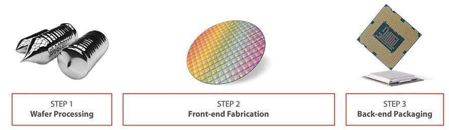
As is often the case, engineered advanced ceramics are behind the scenes—enabling the impressive semiconductor fabrication process by delivering consistent performance despite stringent thermal, chemical, electrical, mechanical, dimensional, and cleanliness requirements. These complex integrated circuits are built one layer at a time on semiconducting wafers (typically silicon), in some of the most aggressive and challenging environments. Sophisticated semiconductor processing equipment is designed to deposit, pattern, etch, and anneal numerous layers of tailored dielectric and metal materials using highly reactive gasses, corrosive liquids, powerful plasma, and dramatic temperature changes. Advanced ceramics are among the only materials that can be engineered to endure hundreds of aggressive cycles in these harsh environments while delivering clean, consistent performance.
Semiconductor equipment manufacturers are increasingly taking advantage of the unique properties of ceramics in each of these stages—leveraging mechanical, chemical, thermal, and electrical performance to handle wafers for better yields, to accelerate processing for higher throughput, and to extend the useful life of equipment for lower operating costs. Taking a closer look at some examples will demonstrate how engineered ceramics enable a variety of semiconductor processes.
View the full article at Ceramic Industry!